

source:Industry News release time:2022-08-26 Article author:yu Popular:pcb
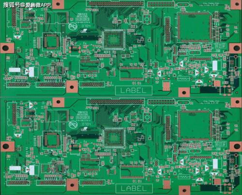
PCB circuit board design solder joints are too dense, it is easy to cause continuous wave soldering and leakage between solder joints. Below, the editor of Zhongke circuit board manufacturer will analyze the optimization method of excessively dense solder joints in PCB circuit board design.
Analysis of the optimization method of excessively dense solder joints in PCB circuit board design
Analysis: This board has many plug-in components and is relatively dense. Because the spacing between the solder joints is 0.3-0.5mm, it is easy to cause continuous welding, and at the same time, due to the poor quality of the flux, a large amount of electricity leakage occurs in the rainy weather in the south.
Countermeasures: Increase the spacing between solder joints and add solder mask oil in the middle. Strictly control flux quality.
Thinking: When designing a denser PCB circuit board, try to make it denser in a small area, and open the place that can be opened as much as possible. For example, although the safe spacing of the PCB circuit board is 0.3MM, the place where 0.6MM can be achieved should be increased to more than 0.6 as much as possible, so that the probability of problems will be greatly reduced.
Read recommendations:
Six-layer Immersion Gold Board (BGA)
Popular recommended products
High frequency PCB
2021-04-27Six-layer Immersion Gold Board (BGA)
2021-05-27Six-layer Immersion Gold Board (BGA)
2021-05-24Six-layer Immersion Gold Board (BGA)
2021-04-27Aluminum substrate (double-sided)
2021-04-27Six-layer Immersion Gold Board (BGA)
2021-05-27Six-layer Immersion Gold Board (BGA)
2021-04-27Network communication board (sixth floor)
2021-04-29Mobile phone template (six layers)
2021-04-27Single copper base PCB
2021-04-27Six-layer Immersion Gold Board (BGA)
2021-04-27High frequency PCB
2021-04-27Silver oil perforated plate (double-sided)
2021-04-27Six-layer Immersion Gold Board (BGA)
2021-05-27High frequency PCB
2021-04-27Computer card board (four layers)
2021-04-25Display board (six layers)
2021-04-27Single-sided double-layer AL base PCB
2021-04-27Six-layer Immersion Gold Board (BGA)
2021-04-27High frequency PCB
2021-04-27Laminate copper-based PCB after 4L (sample)
2021-04-27Six-layer Immersion Gold Board (BGA)
2021-05-24Six-layer Immersion Gold Board (BGA)
2021-05-27DIP plugin
2021-05-27Six-layer Immersion Gold Board (BGA)
2021-04-26DIP plugin
2021-05-27SMT stickers
2021-05-27Mobile phone board
2021-04-27Six-layer Immersion Gold Board (BGA)
2021-04-26Six-layer Immersion Gold Board (BGA)
2021-04-26Six-layer Immersion Gold Board (BGA)
2021-04-26Six-layer Immersion Gold Board (BGA)
2021-04-26SMT stickers
2021-05-27Mobile phone board
2021-05-27Related Information
The relationship between PCB safety distance and voltage
2024-04-22SMT surface mount processing.Hybrid circuit board PCB
2024-04-15PCB enterprises should pay attention to SMT matters.Electronic components PCB
2024-04-03PCB - the core building block of electronic products.Automotive Electronics PCB
2024-03-25PCB - the bridge and link of the electronic world
2024-03-18How to define high-frequency and high-precision circuit boards.Industrial Electronics PCB
2024-03-11USB PCB interface layout and wiring requirements
2024-01-22Electrolytic capacitor PCB.Steps for using PCB pins
2024-01-15Automotive ElectronicWhat aspects should be considered when processing and manufacturing PCB boards?
2024-01-08Electrolytic capaciWhat is the difference between a gold-plated circuit board and a gold-plated one?
2023-12-25When grinding PCB boards, attention should be paid to.Oscillator (belonging to crystal) PCB
2023-12-18Industrial Electronics PCB!What precautions should be taken when copying and grinding PCB boards
2023-12-11Do you know who is more suitable for LED direct display, regarding the difference between PCB board
2023-12-05Aluminum electrolytic capacitor PCB.What are the standards for selecting PCB boards
2023-11-27Surface Mount Technology (SMT) Phase PCB
2023-11-20Oscillator (belonging to crystal) PCB.The main functions of PCB board
2023-11-13What is the difference between RO filter and PCB filter
2023-11-06Method for determining blind hole PCB board
2023-11-01Electronic Manufacturing Services PCB!What are the effects of PCB board color on performance?
2023-10-23Introduction to the Manufacturing Steps and Requirements of PCBA Test Stand
2023-10-16PCB version maturity stage.AOI circuit board price
2023-09-25How to maintain a PCB circuit board
2023-09-19Development Trend of Printed Circuit Board.Zener diode PCB Vendor
2023-09-14Common problems and cause analysis of PCB circuit board sampling.Zener diode PCB price
2023-09-08What are the issues that need to be understood in PCB circuit board design?IGBT module PCB factory
2023-09-08How to reduce the risk of bending and deformation in PCB circuit board production?Inverter PCB Produ
2023-08-16What are the three main factors that constitute welding defects in PCB circuit boards?Multilayer PCB
2023-08-16The structure of a glass teapot.LCD Module PCB factory
2023-08-11Glass teapot.Inverter PCB Processing
2023-08-11PCB online debugging
2023-08-08
CopyRight © 2007-2024Shenzhen Weienchen Technology Co., Ltd.
粤ICP备2021061255号

Address:
1205, Floor 12, Building 3, Chuangyi Office Building, No. 110, Ziheng West Road, Jinsha Community, Kengzi Street, Pingshan District, Shenzhen, Guangdong, China

Tel:
+86-755-29662580

Email:
sales@victoriapcb.com

PCB

PCBA
Service
Process
 Tel: +86-755-29662580
 Email: sales@victoriapcb.com
 中
中 current position:


