

source:Industry News release time:2021-09-13 Article author:sznbone Popular:pcb
Almost all printed circuits are required to be printed on the PCB circuit board, with names to identify components, circuits, test points and the printed board itself. The circuit board factory also attaches great importance to this aspect. With curiosity, we walked into the circuit board factory to understand the little knowledge related to printed circuit signs and identification.
In the production of PCB circuit boards, the name can be printed after the printed board is etched, or etched out at the same time as the circuit is etched. If it is printed later, it is usually printed with a silk screen omission process, or stamped with a stamp. In either case, in order to ensure the electrical and chemical properties, the marking material must be carefully selected. Taking into account this principle and some additional process steps involved, usually the designer must have a name on its photographic base map, and etch it out at the same time as the circuit is etched. Although these names are conductive, they generally do not cause problems. The handwriting of the names should be small enough to withstand etching and be clearly visible. The thickness of the copper foil and the position of the name relative to the wire will determine how much the name will be damaged during etching. When using 2 ounces of 3 ounces of copper foil, the name is not clear when it is made very small.
PCB circuit board
In order to facilitate the testing and maintenance of a printed board assembly, as well as to facilitate the visual inspection of the assembly with drawings and data, the reference name mark of the component should be considered. In addition to the reference name sign, the polarity of capacitors and diodes should be pointed out, and they should be marked as close as possible to their mounting holes. The reference name and polarity should be completely visible where the components are placed. The No. 1 lead of the dual in-line integrated circuit should always be marked, and the TO-5 type integrated circuit with the 6, 8, 10 or 12 lead should also be marked.
Printed circuit boards should have two identification marks of different nature, because before the assembly of electrical components, the manufacturer has to machine and plate the printed board, which requires the use of documents and a method of identifying the printed board. One is the manufacturing drawing number of the printed PCB circuit board (original drawing number), and the other is the number of the printed PCB circuit board assembly should also be marked on the component side. The electrical components are assembled on this component side and replaced Spare components are usually tested and repaired here. The number should always be edited by pressing "ASSYNO". In addition, in order to find, the printed board assembly must be numbered consecutively. If space permits, your company name can be displayed on the printed board. All these requirements are easy to do with the etching foil method.
Read recommendations:
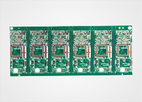
Network communication board (sixth floor)
The role of FPC flexible circuit board solder mask.Electronic components PCB
Popular recommended products
High frequency PCB
2021-04-27High frequency PCB
2021-04-27Mobile phone template (six layers)
2021-04-27Six-layer Immersion Gold Board (BGA)
2021-04-27Single-sided double-layer AL base PCB
2021-04-27Aluminum substrate (double-sided)
2021-04-27Silver oil perforated plate (double-sided)
2021-04-27Six-layer Immersion Gold Board (BGA)
2021-05-27Single copper base PCB
2021-04-27Six-layer Immersion Gold Board (BGA)
2021-04-27Six-layer Immersion Gold Board (BGA)
2021-05-27Six-layer Immersion Gold Board (BGA)
2021-05-24Six-layer Immersion Gold Board (BGA)
2021-05-24Six-layer Immersion Gold Board (BGA)
2021-05-27High frequency PCB
2021-04-27Six-layer Immersion Gold Board (BGA)
2021-04-27Display board (six layers)
2021-04-27Laminate copper-based PCB after 4L (sample)
2021-04-27High frequency PCB
2021-04-27Network communication board (sixth floor)
2021-04-29Computer card board (four layers)
2021-04-25Six-layer Immersion Gold Board (BGA)
2021-04-27Six-layer Immersion Gold Board (BGA)
2021-05-27Six-layer Immersion Gold Board (BGA)
2021-04-26DIP plugin
2021-05-27Six-layer Immersion Gold Board (BGA)
2021-04-26Mobile phone board
2021-04-27Six-layer Immersion Gold Board (BGA)
2021-04-26Six-layer Immersion Gold Board (BGA)
2021-04-26SMT stickers
2021-05-27SMT stickers
2021-05-27DIP plugin
2021-05-27Mobile phone board
2021-05-27Six-layer Immersion Gold Board (BGA)
2021-04-26Related Information
The relationship between PCB safety distance and voltage
2024-04-22SMT surface mount processing.Hybrid circuit board PCB
2024-04-15PCB enterprises should pay attention to SMT matters.Electronic components PCB
2024-04-03PCB - the core building block of electronic products.Automotive Electronics PCB
2024-03-25PCB - the bridge and link of the electronic world
2024-03-18How to define high-frequency and high-precision circuit boards.Industrial Electronics PCB
2024-03-11USB PCB interface layout and wiring requirements
2024-01-22Electrolytic capacitor PCB.Steps for using PCB pins
2024-01-15Automotive ElectronicWhat aspects should be considered when processing and manufacturing PCB boards?
2024-01-08Electrolytic capaciWhat is the difference between a gold-plated circuit board and a gold-plated one?
2023-12-25When grinding PCB boards, attention should be paid to.Oscillator (belonging to crystal) PCB
2023-12-18Industrial Electronics PCB!What precautions should be taken when copying and grinding PCB boards
2023-12-11Do you know who is more suitable for LED direct display, regarding the difference between PCB board
2023-12-05Aluminum electrolytic capacitor PCB.What are the standards for selecting PCB boards
2023-11-27Surface Mount Technology (SMT) Phase PCB
2023-11-20Oscillator (belonging to crystal) PCB.The main functions of PCB board
2023-11-13What is the difference between RO filter and PCB filter
2023-11-06Method for determining blind hole PCB board
2023-11-01Electronic Manufacturing Services PCB!What are the effects of PCB board color on performance?
2023-10-23Introduction to the Manufacturing Steps and Requirements of PCBA Test Stand
2023-10-16PCB version maturity stage.AOI circuit board price
2023-09-25How to maintain a PCB circuit board
2023-09-19Development Trend of Printed Circuit Board.Zener diode PCB Vendor
2023-09-14Common problems and cause analysis of PCB circuit board sampling.Zener diode PCB price
2023-09-08What are the issues that need to be understood in PCB circuit board design?IGBT module PCB factory
2023-09-08How to reduce the risk of bending and deformation in PCB circuit board production?Inverter PCB Produ
2023-08-16What are the three main factors that constitute welding defects in PCB circuit boards?Multilayer PCB
2023-08-16The structure of a glass teapot.LCD Module PCB factory
2023-08-11Glass teapot.Inverter PCB Processing
2023-08-11PCB online debugging
2023-08-08
CopyRight © 2007-2024Shenzhen Weienchen Technology Co., Ltd.
粤ICP备2021061255号

Address:
1205, Floor 12, Building 3, Chuangyi Office Building, No. 110, Ziheng West Road, Jinsha Community, Kengzi Street, Pingshan District, Shenzhen, Guangdong, China

Tel:
+86-755-29662580

Email:
sales@victoriapcb.com

PCB

PCBA
Service
Process
 Tel: +86-755-29662580
 Email: sales@victoriapcb.com
 中
中 current position:


