

source:Industry News release time:2023-02-20 Article author:yu Popular:pcb
1. The first choice to create a new project. Method: It is necessary to start the Protel99se software, and then create a new engineering project by ordering the menu. The project is best named after its own name or school number to choose the preservation path.
2. Create a new schematic map editor and print circuit board editor. Methods: Create a new schematic graph editor and print circuit board editor in the document manager), and then enter the scratch of the drawer to set the drawer.
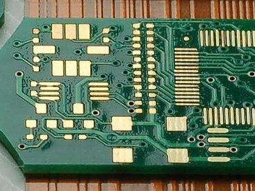
circuit board
3. Place the components and draw the line. Methods: Select components in the gallery in the gallery according to the given circuit diagram and place them in the schematic editor, then layout the component, and finally save and save it.
4. Pay attention to the steps of the CAD drawing PCB board circuit diagram, use the command of the wire when drawing the wire; the command of the bus should be used when drawing the bus; Function, this is also the basic point for students to master.
5. Update the device running number, and perform ERC to detect the painted circuit schematic diagram. This step also needs to choose the correct command for operation.
6. Package the components. Methods: Open the printed circuit board editor that has been established in advance before packaging, and find the corresponding packaging in the component library. Common component packaging: resistance, non -polar capacitors, polar capacitors, diodes, triode, and dual -column direct -inserted components are prefixed by DIP, and the packaging of the interface device is based on SIP.
7. Generate network tables. How to do this step? Boyuan Electronic designer said that the CreatenetList command can be created by the DESIGN drop -down menu or click the mouse to right -click to select the CreatenetList command.
Read recommendations:
Six-layer Immersion Gold Board (BGA)
Six-layer Immersion Gold Board (BGA)
Six-layer Immersion Gold Board (BGA)
Gigabit Ethernet PCB Layout Guidelines.Aluminum electrolytic capacitor PCB
Popular recommended products
High frequency PCB
2021-04-27Six-layer Immersion Gold Board (BGA)
2021-05-27Six-layer Immersion Gold Board (BGA)
2021-04-27Six-layer Immersion Gold Board (BGA)
2021-05-24High frequency PCB
2021-04-27Six-layer Immersion Gold Board (BGA)
2021-04-27Aluminum substrate (double-sided)
2021-04-27Six-layer Immersion Gold Board (BGA)
2021-05-27Mobile phone template (six layers)
2021-04-27Six-layer Immersion Gold Board (BGA)
2021-04-27Laminate copper-based PCB after 4L (sample)
2021-04-27Single-sided double-layer AL base PCB
2021-04-27Six-layer Immersion Gold Board (BGA)
2021-05-27Six-layer Immersion Gold Board (BGA)
2021-05-27Network communication board (sixth floor)
2021-04-29High frequency PCB
2021-04-27Silver oil perforated plate (double-sided)
2021-04-27High frequency PCB
2021-04-27Computer card board (four layers)
2021-04-25Single copper base PCB
2021-04-27Display board (six layers)
2021-04-27Six-layer Immersion Gold Board (BGA)
2021-04-27Six-layer Immersion Gold Board (BGA)
2021-05-24DIP plugin
2021-05-27Six-layer Immersion Gold Board (BGA)
2021-04-26Six-layer Immersion Gold Board (BGA)
2021-04-26SMT stickers
2021-05-27Mobile phone board
2021-04-27Six-layer Immersion Gold Board (BGA)
2021-04-26DIP plugin
2021-05-27SMT stickers
2021-05-27Six-layer Immersion Gold Board (BGA)
2021-04-26Mobile phone board
2021-05-27Six-layer Immersion Gold Board (BGA)
2021-04-26Related Information
The relationship between PCB safety distance and voltage
2024-04-22SMT surface mount processing.Hybrid circuit board PCB
2024-04-15PCB enterprises should pay attention to SMT matters.Electronic components PCB
2024-04-03PCB - the core building block of electronic products.Automotive Electronics PCB
2024-03-25PCB - the bridge and link of the electronic world
2024-03-18How to define high-frequency and high-precision circuit boards.Industrial Electronics PCB
2024-03-11USB PCB interface layout and wiring requirements
2024-01-22Electrolytic capacitor PCB.Steps for using PCB pins
2024-01-15Automotive ElectronicWhat aspects should be considered when processing and manufacturing PCB boards?
2024-01-08Electrolytic capaciWhat is the difference between a gold-plated circuit board and a gold-plated one?
2023-12-25When grinding PCB boards, attention should be paid to.Oscillator (belonging to crystal) PCB
2023-12-18Industrial Electronics PCB!What precautions should be taken when copying and grinding PCB boards
2023-12-11Do you know who is more suitable for LED direct display, regarding the difference between PCB board
2023-12-05Aluminum electrolytic capacitor PCB.What are the standards for selecting PCB boards
2023-11-27Surface Mount Technology (SMT) Phase PCB
2023-11-20Oscillator (belonging to crystal) PCB.The main functions of PCB board
2023-11-13What is the difference between RO filter and PCB filter
2023-11-06Method for determining blind hole PCB board
2023-11-01Electronic Manufacturing Services PCB!What are the effects of PCB board color on performance?
2023-10-23Introduction to the Manufacturing Steps and Requirements of PCBA Test Stand
2023-10-16PCB version maturity stage.AOI circuit board price
2023-09-25How to maintain a PCB circuit board
2023-09-19Development Trend of Printed Circuit Board.Zener diode PCB Vendor
2023-09-14Common problems and cause analysis of PCB circuit board sampling.Zener diode PCB price
2023-09-08What are the issues that need to be understood in PCB circuit board design?IGBT module PCB factory
2023-09-08How to reduce the risk of bending and deformation in PCB circuit board production?Inverter PCB Produ
2023-08-16What are the three main factors that constitute welding defects in PCB circuit boards?Multilayer PCB
2023-08-16The structure of a glass teapot.LCD Module PCB factory
2023-08-11Glass teapot.Inverter PCB Processing
2023-08-11PCB online debugging
2023-08-08
CopyRight © 2007-2024Shenzhen Weienchen Technology Co., Ltd.
粤ICP备2021061255号

Address:
1205, Floor 12, Building 3, Chuangyi Office Building, No. 110, Ziheng West Road, Jinsha Community, Kengzi Street, Pingshan District, Shenzhen, Guangdong, China

Tel:
+86-755-29662580

Email:
sales@victoriapcb.com

PCB

PCBA
Service
Process
 Tel: +86-755-29662580
 Email: sales@victoriapcb.com
 中
中 current position:


