

source:Industry News release time:2022-04-20 Article author:yu Popular:pcb
Circuit board, the full name of printed circuit board, is a bridge for signal communication between high-tech, among which there is an industrial control board that connects switches and machinery. A circle of vias and copper tapes are placed around the board, and even some RF boards will be metallized and wrapped around the board. Many small partners do not understand why they do this. Is it an engineer showing off technology and doing useless work?
In fact, it is not, it is naturally purposeful. Nowadays, with the improvement of system speed, not only the timing and signal integrity of high-speed signals are prominent, but also the EMC problems caused by electromagnetic interference and power integrity of high-speed digital signals in the system are also very prominent. The electromagnetic interference generated by high-speed digital signals will not only cause serious mutual interference inside the system and reduce the anti-interference ability of the system, but also generate strong electromagnetic radiation in the external space, causing the electromagnetic radiation emission of the system to seriously exceed the EMC standard, making the circuit The products of board manufacturers cannot pass the EMC standard certification. The edge radiation of the multilayer PCB is a relatively common source of electromagnetic radiation. Edge radiation occurs when unexpected currents reach the edges of the ground and power planes, with ground and power noise that manifests as: Insufficient power bypassing. The cylindrical radiated magnetic field generated by the inductive via radiates between the layers of the circuit board and eventually meets at the edge of the circuit board. Stripline return currents that carry high frequency signals are too close to the edge of the board. In order to prevent these situations from occurring, a circle of ground vias are punched around the PCB with a 1/20 wavelength hole spacing to form a ground via shield to prevent TME waves from radiating externally.
For microwave circuit boards, the wavelength is further reduced, and due to the current PCB production process, the spacing between holes cannot be made very small. At this time, the spacing of 1/20 wavelength is shielded by holes around the PCB. The effect of the microwave board is not very obvious. At this time, it is necessary to use the PCB version metallization wrapping process to surround the entire edge of the board with metal, so that the microwave signal cannot be radiated from the edge of the PCB board. Of course, the edge metallization package is used. The edge process will also lead to a lot of increase in the manufacturing cost of the PCB. For RF microwave boards, some sensitive circuits, and circuits with strong radiation sources can design a shielding cavity soldered on the PCB. The PCB circuit board should be designed with a "via-hole shielding wall", that is, on the PCB and shielding. The part where the cavity wall is close to the ground is added with a grounded via. This forms a relatively isolated area. After confirmation, it can be sent to the multi-layer circuit board manufacturer for production.
Read recommendations:
Network communication board (sixth floor)
Popular recommended products
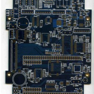
Six-layer Immersion Gold Board (BGA)
2021-05-27Silver oil perforated plate (double-sided)
2021-04-27Single-sided double-layer AL base PCB
2021-04-27Six-layer Immersion Gold Board (BGA)
2021-04-27Aluminum substrate (double-sided)
2021-04-27High frequency PCB
2021-04-27Six-layer Immersion Gold Board (BGA)
2021-04-27Computer card board (four layers)
2021-04-25Display board (six layers)
2021-04-27Network communication board (sixth floor)
2021-04-29Six-layer Immersion Gold Board (BGA)
2021-04-27Six-layer Immersion Gold Board (BGA)
2021-05-27Six-layer Immersion Gold Board (BGA)
2021-05-24High frequency PCB
2021-04-27Six-layer Immersion Gold Board (BGA)
2021-05-27Six-layer Immersion Gold Board (BGA)
2021-04-27Single copper base PCB
2021-04-27Six-layer Immersion Gold Board (BGA)
2021-05-27Laminate copper-based PCB after 4L (sample)
2021-04-27High frequency PCB
2021-04-27High frequency PCB
2021-04-27Mobile phone template (six layers)
2021-04-27Six-layer Immersion Gold Board (BGA)
2021-05-24DIP plugin
2021-05-27Mobile phone board
2021-05-27SMT stickers
2021-05-27DIP plugin
2021-05-27Six-layer Immersion Gold Board (BGA)
2021-04-26Six-layer Immersion Gold Board (BGA)
2021-04-26Six-layer Immersion Gold Board (BGA)
2021-04-26Mobile phone board
2021-04-27Six-layer Immersion Gold Board (BGA)
2021-04-26SMT stickers
2021-05-27Six-layer Immersion Gold Board (BGA)
2021-04-26Related Information
The relationship between PCB safety distance and voltage
2024-04-22SMT surface mount processing.Hybrid circuit board PCB
2024-04-15PCB enterprises should pay attention to SMT matters.Electronic components PCB
2024-04-03PCB - the core building block of electronic products.Automotive Electronics PCB
2024-03-25PCB - the bridge and link of the electronic world
2024-03-18How to define high-frequency and high-precision circuit boards.Industrial Electronics PCB
2024-03-11USB PCB interface layout and wiring requirements
2024-01-22Electrolytic capacitor PCB.Steps for using PCB pins
2024-01-15Automotive ElectronicWhat aspects should be considered when processing and manufacturing PCB boards?
2024-01-08Electrolytic capaciWhat is the difference between a gold-plated circuit board and a gold-plated one?
2023-12-25When grinding PCB boards, attention should be paid to.Oscillator (belonging to crystal) PCB
2023-12-18Industrial Electronics PCB!What precautions should be taken when copying and grinding PCB boards
2023-12-11Do you know who is more suitable for LED direct display, regarding the difference between PCB board
2023-12-05Aluminum electrolytic capacitor PCB.What are the standards for selecting PCB boards
2023-11-27Surface Mount Technology (SMT) Phase PCB
2023-11-20Oscillator (belonging to crystal) PCB.The main functions of PCB board
2023-11-13What is the difference between RO filter and PCB filter
2023-11-06Method for determining blind hole PCB board
2023-11-01Electronic Manufacturing Services PCB!What are the effects of PCB board color on performance?
2023-10-23Introduction to the Manufacturing Steps and Requirements of PCBA Test Stand
2023-10-16PCB version maturity stage.AOI circuit board price
2023-09-25How to maintain a PCB circuit board
2023-09-19Development Trend of Printed Circuit Board.Zener diode PCB Vendor
2023-09-14Common problems and cause analysis of PCB circuit board sampling.Zener diode PCB price
2023-09-08What are the issues that need to be understood in PCB circuit board design?IGBT module PCB factory
2023-09-08How to reduce the risk of bending and deformation in PCB circuit board production?Inverter PCB Produ
2023-08-16What are the three main factors that constitute welding defects in PCB circuit boards?Multilayer PCB
2023-08-16The structure of a glass teapot.LCD Module PCB factory
2023-08-11Glass teapot.Inverter PCB Processing
2023-08-11PCB online debugging
2023-08-08
CopyRight © 2007-2024Shenzhen Weienchen Technology Co., Ltd.
粤ICP备2021061255号

Address:
1205, Floor 12, Building 3, Chuangyi Office Building, No. 110, Ziheng West Road, Jinsha Community, Kengzi Street, Pingshan District, Shenzhen, Guangdong, China

Tel:
+86-755-29662580

Email:
sales@victoriapcb.com

PCB

PCBA
Service
Process
 Tel: +86-755-29662580
 Email: sales@victoriapcb.com
 中
中 current position:


