

source:Industry News release time:2023-08-16 Article author:yu Popular:pcb
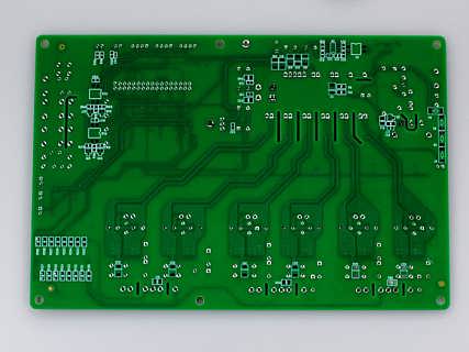
PCB circuit boards are prone to solder back problems during the production process, causing bending and warping of the board, which affects the product qualification rate. So, how to reduce the risk of bending and deformation in PCB circuit board production?
1. The effect of reducing temperature on the stress of PCB circuit boards. Due to temperature being the main source of stress on circuit boards, as long as the temperature of the reflow furnace is reduced or the production heating speed of the circuit board in the welding furnace is slowed down, the bending and warping of the board can be greatly reduced.
2. The use of boards with higher Tg can increase their ability to withstand stress deformation, but the production cost of circuit boards is also relatively high.
3. Increase the thickness of the PCB circuit board. Many electronic products have circuit board thicknesses of 1.0mm, 0.8mm, or 0.6mm for lighter purposes. It is recommended that if there are no requirements, the circuit board should be 1.6mm thick, which can greatly reduce the risk of bending and deformation of the board.
4. Reduce the size of the circuit board and reduce the number of plywood. Due to the fact that most welding furnaces use chains to drive the circuit board forward, the circuit board may sag and deform in the back welding furnace due to its own weight. Therefore, it is advisable to use the circuit board as the edge of the back welding board to reduce the sagging deformation caused by the weight of the circuit board itself.
5. Use furnace holder fixtures. Habitually using a furnace to reduce deformation can reduce plate bending on the furnace. If a single-layer tray cannot reduce the deformation of the circuit board, a cover must be added to clamp the upper and lower layers of the tray together to reduce the deformation problem of the welding furnace above the circuit board.
Read recommendations:
Six-layer Immersion Gold Board (BGA)
Silver oil perforated plate (double-sided)
Six-layer Immersion Gold Board (BGA)
What is the relationship between PCB design and microcontroller
Popular recommended products
Display board (six layers)
2021-04-27Six-layer Immersion Gold Board (BGA)
2021-05-27High frequency PCB
2021-04-27Computer card board (four layers)
2021-04-25High frequency PCB
2021-04-27Six-layer Immersion Gold Board (BGA)
2021-05-24Six-layer Immersion Gold Board (BGA)
2021-04-27Single-sided double-layer AL base PCB
2021-04-27Single copper base PCB
2021-04-27Six-layer Immersion Gold Board (BGA)
2021-05-27Six-layer Immersion Gold Board (BGA)
2021-04-27High frequency PCB
2021-04-27Six-layer Immersion Gold Board (BGA)
2021-04-27Six-layer Immersion Gold Board (BGA)
2021-05-24Six-layer Immersion Gold Board (BGA)
2021-05-27Silver oil perforated plate (double-sided)
2021-04-27Aluminum substrate (double-sided)
2021-04-27Six-layer Immersion Gold Board (BGA)
2021-05-27Mobile phone template (six layers)
2021-04-27Network communication board (sixth floor)
2021-04-29Six-layer Immersion Gold Board (BGA)
2021-04-27High frequency PCB
2021-04-27Laminate copper-based PCB after 4L (sample)
2021-04-27SMT stickers
2021-05-27SMT stickers
2021-05-27DIP plugin
2021-05-27Six-layer Immersion Gold Board (BGA)
2021-04-26Six-layer Immersion Gold Board (BGA)
2021-04-26Six-layer Immersion Gold Board (BGA)
2021-04-26Six-layer Immersion Gold Board (BGA)
2021-04-26Six-layer Immersion Gold Board (BGA)
2021-04-26Mobile phone board
2021-05-27DIP plugin
2021-05-27Mobile phone board
2021-04-27Related Information
The relationship between PCB safety distance and voltage
2024-04-22SMT surface mount processing.Hybrid circuit board PCB
2024-04-15PCB enterprises should pay attention to SMT matters.Electronic components PCB
2024-04-03PCB - the core building block of electronic products.Automotive Electronics PCB
2024-03-25PCB - the bridge and link of the electronic world
2024-03-18How to define high-frequency and high-precision circuit boards.Industrial Electronics PCB
2024-03-11USB PCB interface layout and wiring requirements
2024-01-22Electrolytic capacitor PCB.Steps for using PCB pins
2024-01-15Automotive ElectronicWhat aspects should be considered when processing and manufacturing PCB boards?
2024-01-08Electrolytic capaciWhat is the difference between a gold-plated circuit board and a gold-plated one?
2023-12-25When grinding PCB boards, attention should be paid to.Oscillator (belonging to crystal) PCB
2023-12-18Industrial Electronics PCB!What precautions should be taken when copying and grinding PCB boards
2023-12-11Do you know who is more suitable for LED direct display, regarding the difference between PCB board
2023-12-05Aluminum electrolytic capacitor PCB.What are the standards for selecting PCB boards
2023-11-27Surface Mount Technology (SMT) Phase PCB
2023-11-20Oscillator (belonging to crystal) PCB.The main functions of PCB board
2023-11-13What is the difference between RO filter and PCB filter
2023-11-06Method for determining blind hole PCB board
2023-11-01Electronic Manufacturing Services PCB!What are the effects of PCB board color on performance?
2023-10-23Introduction to the Manufacturing Steps and Requirements of PCBA Test Stand
2023-10-16PCB version maturity stage.AOI circuit board price
2023-09-25How to maintain a PCB circuit board
2023-09-19Development Trend of Printed Circuit Board.Zener diode PCB Vendor
2023-09-14Common problems and cause analysis of PCB circuit board sampling.Zener diode PCB price
2023-09-08What are the issues that need to be understood in PCB circuit board design?IGBT module PCB factory
2023-09-08How to reduce the risk of bending and deformation in PCB circuit board production?Inverter PCB Produ
2023-08-16What are the three main factors that constitute welding defects in PCB circuit boards?Multilayer PCB
2023-08-16The structure of a glass teapot.LCD Module PCB factory
2023-08-11Glass teapot.Inverter PCB Processing
2023-08-11PCB online debugging
2023-08-08
CopyRight © 2007-2024Shenzhen Weienchen Technology Co., Ltd.
粤ICP备2021061255号

Address:
1205, Floor 12, Building 3, Chuangyi Office Building, No. 110, Ziheng West Road, Jinsha Community, Kengzi Street, Pingshan District, Shenzhen, Guangdong, China

Tel:
+86-755-29662580

Email:
sales@victoriapcb.com

PCB

PCBA
Service
Process
 Tel: +86-755-29662580
 Email: sales@victoriapcb.com
 中
中 current position:


