

source:Industry News release time:2022-03-21 Article author:sznbone Popular:pcb
In 1961, Hazelting Corp. of the United States published Multiplanar, which was the pioneer in the development of the first multi-layer board. This method is almost the same as the current method of manufacturing multi-layer boards using the plated-through hole method. After Japan stepped into this field in 1963, various ideas and manufacturing methods for multi-layer boards have gradually become popular all over the world. With the transition from transistors to the era of integrated circuits, the application of computers has gradually become common, and due to the demand for high functionality, large wiring capacity and good transmission characteristics have become the focus of multi-layer boards.
At first, three manufacturing methods of multi-layer boards were disclosed by the clearance method (Clearance Hole) method, the build-up method (Build Up) method, and the plating-through method (PTH) method. Since the mesoporous method is labor-intensive and limited in high density, it has not been put into practical use. The build-up method has been unknown because of its complex manufacturing method and the advantages of high density, but because the demand for high density was not as urgent as it is now, it has been unknown. Recently, due to the increasing demand for high density circuit boards, it has been Become the focus of research and development of various manufacturers. As for the PTH method, which has the same process as the double-sided panel, it is still the mainstream manufacturing method for multi-layer boards.
The production method of multi-layer boards is generally made by the inner layer pattern first, and then the single-sided or double-sided substrate is made by printing and etching method, and is incorporated into the designated interlayer, and then heated, pressurized and bonded. As for the subsequent drilling The hole is the same as the plated-through hole method of the double-sided board. These basic manufacturing methods have not changed much from those dating back to the 1960s. However, as materials and process technologies (eg: press-bonding technology, solving slag during drilling, and film improvement) have become more mature, the attached The characteristics of pre-multilayer boards are more diverse.
Read recommendations:
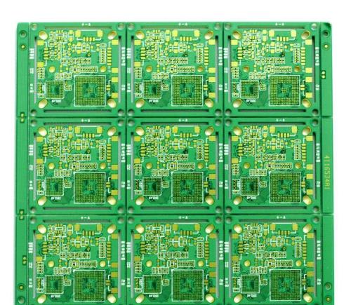
Six-layer Immersion Gold Board (BGA)
Six-layer Immersion Gold Board (BGA)
Popular recommended products
Six-layer Immersion Gold Board (BGA)
2021-05-24High frequency PCB
2021-04-27Aluminum substrate (double-sided)
2021-04-27Six-layer Immersion Gold Board (BGA)
2021-04-27Display board (six layers)
2021-04-27Six-layer Immersion Gold Board (BGA)
2021-04-27High frequency PCB
2021-04-27Six-layer Immersion Gold Board (BGA)
2021-05-27High frequency PCB
2021-04-27Mobile phone template (six layers)
2021-04-27High frequency PCB
2021-04-27Six-layer Immersion Gold Board (BGA)
2021-04-27Computer card board (four layers)
2021-04-25Single copper base PCB
2021-04-27Network communication board (sixth floor)
2021-04-29Six-layer Immersion Gold Board (BGA)
2021-05-27Six-layer Immersion Gold Board (BGA)
2021-05-27Six-layer Immersion Gold Board (BGA)
2021-05-27Single-sided double-layer AL base PCB
2021-04-27Silver oil perforated plate (double-sided)
2021-04-27Laminate copper-based PCB after 4L (sample)
2021-04-27Six-layer Immersion Gold Board (BGA)
2021-04-27Six-layer Immersion Gold Board (BGA)
2021-05-24Six-layer Immersion Gold Board (BGA)
2021-04-26Six-layer Immersion Gold Board (BGA)
2021-04-26Six-layer Immersion Gold Board (BGA)
2021-04-26Mobile phone board
2021-04-27Six-layer Immersion Gold Board (BGA)
2021-04-26SMT stickers
2021-05-27SMT stickers
2021-05-27DIP plugin
2021-05-27Six-layer Immersion Gold Board (BGA)
2021-04-26Mobile phone board
2021-05-27DIP plugin
2021-05-27Related Information
The relationship between PCB safety distance and voltage
2024-04-22SMT surface mount processing.Hybrid circuit board PCB
2024-04-15PCB enterprises should pay attention to SMT matters.Electronic components PCB
2024-04-03PCB - the core building block of electronic products.Automotive Electronics PCB
2024-03-25PCB - the bridge and link of the electronic world
2024-03-18How to define high-frequency and high-precision circuit boards.Industrial Electronics PCB
2024-03-11USB PCB interface layout and wiring requirements
2024-01-22Electrolytic capacitor PCB.Steps for using PCB pins
2024-01-15Automotive ElectronicWhat aspects should be considered when processing and manufacturing PCB boards?
2024-01-08Electrolytic capaciWhat is the difference between a gold-plated circuit board and a gold-plated one?
2023-12-25When grinding PCB boards, attention should be paid to.Oscillator (belonging to crystal) PCB
2023-12-18Industrial Electronics PCB!What precautions should be taken when copying and grinding PCB boards
2023-12-11Do you know who is more suitable for LED direct display, regarding the difference between PCB board
2023-12-05Aluminum electrolytic capacitor PCB.What are the standards for selecting PCB boards
2023-11-27Surface Mount Technology (SMT) Phase PCB
2023-11-20Oscillator (belonging to crystal) PCB.The main functions of PCB board
2023-11-13What is the difference between RO filter and PCB filter
2023-11-06Method for determining blind hole PCB board
2023-11-01Electronic Manufacturing Services PCB!What are the effects of PCB board color on performance?
2023-10-23Introduction to the Manufacturing Steps and Requirements of PCBA Test Stand
2023-10-16PCB version maturity stage.AOI circuit board price
2023-09-25How to maintain a PCB circuit board
2023-09-19Development Trend of Printed Circuit Board.Zener diode PCB Vendor
2023-09-14Common problems and cause analysis of PCB circuit board sampling.Zener diode PCB price
2023-09-08What are the issues that need to be understood in PCB circuit board design?IGBT module PCB factory
2023-09-08How to reduce the risk of bending and deformation in PCB circuit board production?Inverter PCB Produ
2023-08-16What are the three main factors that constitute welding defects in PCB circuit boards?Multilayer PCB
2023-08-16The structure of a glass teapot.LCD Module PCB factory
2023-08-11Glass teapot.Inverter PCB Processing
2023-08-11PCB online debugging
2023-08-08
CopyRight © 2007-2024Shenzhen Weienchen Technology Co., Ltd.
粤ICP备2021061255号

Address:
1205, Floor 12, Building 3, Chuangyi Office Building, No. 110, Ziheng West Road, Jinsha Community, Kengzi Street, Pingshan District, Shenzhen, Guangdong, China

Tel:
+86-755-29662580

Email:
sales@victoriapcb.com

PCB

PCBA
Service
Process
 Tel: +86-755-29662580
 Email: sales@victoriapcb.com
 中
中 current position:


