

source:Industry News release time:2022-04-08 Article author:sznbone Popular:pcb
Traditional circuit boards are often divided into single-sided PCB boards, double-sided circuit boards, and PCB multi-layer boards, and PCB multi-layer boards are further divided into single-press and multiple-press structures. This design of course involves some electrical properties and link density issues, but due to the rapid advancement of electronic product technology, these geometries cannot meet the component mounting density and electrical requirements. In order to increase the link density of components, from a geometrical point of view, only by compressing the space of lines and connection points, can more contacts be accommodated in a small space to increase the link density. Of course, multiple components can also be stacked in one position to increase the packing density. Therefore, high-density circuit boards are not only a circuit board technology, but also an issue of electronic packaging and assembly.
In order to improve the connection density of components, from a geometrical point of view, only by compressing the space between lines and connection points, so that more connections can be accommodated in a smaller space, the connection density can be improved. Of course, there is a different idea, that is, multiple different components can be stacked in the same location to increase the density of the construction. Therefore, from a certain point of view, high-density circuit boards are not only a technical problem of circuit boards, but also a problem of electronic assembly and assembly. This aspect is probably worth some effort by the industry to understand.
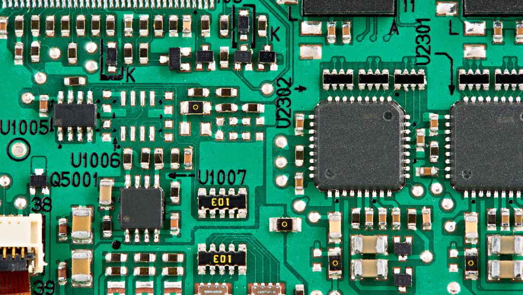
PCB multilayer board
Generally, the so-called electronic package refers to the connection between the semiconductor chip and the carrier board. In this regard, the Civil Road Board Association has published a special book on "electronic component carrier board technology", and those who are interested can refer to it. As for the electronic assembly part, it is the work of re-installing the components after the electronic assembly is completed on another functional circuit board. This connection, generally called OLB (outerleadbond), refers to the connection part of the outer pins of the component. The connection of this part is directly related to the surface contact density of electronic components. When the functions and integration of electronic products are getting higher and higher, and at the same time, the demand for mobility, thinness and multi-functionality is constantly pushed up. , of course there will be high densification pressure.
If a high-density circuit board design concept is adopted, electronic products can gain the following benefits:
1. The high-density circuit board structure adopts a thinner dielectric thickness, and the potential inductance is relatively low.
2. The micro-hole has a low aspect ratio, and the signal transmission reliability is higher than that of the general through-hole.
3. Micro holes can improve the flexibility of circuit configuration and make circuit design easier.
4. The same product design can reduce the number of carrier layers, increase the density and reduce the cost.
5. The use of micro-hole interconnection can shorten the contact distance, reduce signal reflection, and crosstalk between lines, and the components can have better electrical properties and signal accuracy.
6. Increase the wiring density and increase the line capacity per unit area with micro-hole thin lines, which can meet the assembly requirements of high-density contact components, and is conducive to the use of advanced assembly.
7. High-density circuit board micro-via technology allows the carrier board design to shorten the distance between grounding and signal layers, thereby improving RF/electromagnetic wave/electrostatic discharge (RFI/EMI/ESD) interference. The number of grounding wires can be increased to prevent the damage of components caused by instantaneous discharge due to static electricity accumulation.
Modern and popular electronic products should not only have the characteristics of mobility and power saving, but also have no burden to wear and look beautiful. Of course, the most important thing is that they are affordable and can be replaced with fashion.
Read recommendations:
Six-layer Immersion Gold Board (BGA)
Popular recommended products
High frequency PCB
2021-04-27Six-layer Immersion Gold Board (BGA)
2021-04-27High frequency PCB
2021-04-27Six-layer Immersion Gold Board (BGA)
2021-04-27Single-sided double-layer AL base PCB
2021-04-27Network communication board (sixth floor)
2021-04-29Mobile phone template (six layers)
2021-04-27Silver oil perforated plate (double-sided)
2021-04-27Laminate copper-based PCB after 4L (sample)
2021-04-27Aluminum substrate (double-sided)
2021-04-27High frequency PCB
2021-04-27Six-layer Immersion Gold Board (BGA)
2021-04-27Display board (six layers)
2021-04-27Computer card board (four layers)
2021-04-25Six-layer Immersion Gold Board (BGA)
2021-05-27Single copper base PCB
2021-04-27High frequency PCB
2021-04-27Six-layer Immersion Gold Board (BGA)
2021-05-24Six-layer Immersion Gold Board (BGA)
2021-05-27Six-layer Immersion Gold Board (BGA)
2021-05-24Six-layer Immersion Gold Board (BGA)
2021-05-27Six-layer Immersion Gold Board (BGA)
2021-05-27Six-layer Immersion Gold Board (BGA)
2021-04-27Six-layer Immersion Gold Board (BGA)
2021-04-26Six-layer Immersion Gold Board (BGA)
2021-04-26Six-layer Immersion Gold Board (BGA)
2021-04-26Six-layer Immersion Gold Board (BGA)
2021-04-26Mobile phone board
2021-05-27SMT stickers
2021-05-27DIP plugin
2021-05-27Mobile phone board
2021-04-27SMT stickers
2021-05-27Six-layer Immersion Gold Board (BGA)
2021-04-26DIP plugin
2021-05-27Related Information
The relationship between PCB safety distance and voltage
2024-04-22SMT surface mount processing.Hybrid circuit board PCB
2024-04-15PCB enterprises should pay attention to SMT matters.Electronic components PCB
2024-04-03PCB - the core building block of electronic products.Automotive Electronics PCB
2024-03-25PCB - the bridge and link of the electronic world
2024-03-18How to define high-frequency and high-precision circuit boards.Industrial Electronics PCB
2024-03-11USB PCB interface layout and wiring requirements
2024-01-22Electrolytic capacitor PCB.Steps for using PCB pins
2024-01-15Automotive ElectronicWhat aspects should be considered when processing and manufacturing PCB boards?
2024-01-08Electrolytic capaciWhat is the difference between a gold-plated circuit board and a gold-plated one?
2023-12-25When grinding PCB boards, attention should be paid to.Oscillator (belonging to crystal) PCB
2023-12-18Industrial Electronics PCB!What precautions should be taken when copying and grinding PCB boards
2023-12-11Do you know who is more suitable for LED direct display, regarding the difference between PCB board
2023-12-05Aluminum electrolytic capacitor PCB.What are the standards for selecting PCB boards
2023-11-27Surface Mount Technology (SMT) Phase PCB
2023-11-20Oscillator (belonging to crystal) PCB.The main functions of PCB board
2023-11-13What is the difference between RO filter and PCB filter
2023-11-06Method for determining blind hole PCB board
2023-11-01Electronic Manufacturing Services PCB!What are the effects of PCB board color on performance?
2023-10-23Introduction to the Manufacturing Steps and Requirements of PCBA Test Stand
2023-10-16PCB version maturity stage.AOI circuit board price
2023-09-25How to maintain a PCB circuit board
2023-09-19Development Trend of Printed Circuit Board.Zener diode PCB Vendor
2023-09-14Common problems and cause analysis of PCB circuit board sampling.Zener diode PCB price
2023-09-08What are the issues that need to be understood in PCB circuit board design?IGBT module PCB factory
2023-09-08How to reduce the risk of bending and deformation in PCB circuit board production?Inverter PCB Produ
2023-08-16What are the three main factors that constitute welding defects in PCB circuit boards?Multilayer PCB
2023-08-16The structure of a glass teapot.LCD Module PCB factory
2023-08-11Glass teapot.Inverter PCB Processing
2023-08-11PCB online debugging
2023-08-08
CopyRight © 2007-2024Shenzhen Weienchen Technology Co., Ltd.
粤ICP备2021061255号

Address:
1205, Floor 12, Building 3, Chuangyi Office Building, No. 110, Ziheng West Road, Jinsha Community, Kengzi Street, Pingshan District, Shenzhen, Guangdong, China

Tel:
+86-755-29662580

Email:
sales@victoriapcb.com

PCB

PCBA
Service
Process
 Tel: +86-755-29662580
 Email: sales@victoriapcb.com
 中
中 current position:


