
source:Optimization dedicated release time:2022-04-18 Article author:yu Popular:pcb
High-precision circuit board refers to the use of fine line width/spacing, tiny holes, narrow ring width (or no ring width), buried and blind holes and other technologies to achieve high density. And high precision means that the result of "thin, small, narrow, thin" will inevitably bring high precision requirements. Take the line width as an example: O.20mm line width, according to the regulations, the production of O.16 ~ 0.24mm is qualified, and its The error is (O.20±0.04)mm; and the line width of O.10mm, the same error is (0.10±O.02)mm, obviously the accuracy of the latter is doubled, and so on is not difficult to understand, The high precision requirements are therefore not discussed separately. But it is a prominent problem in production technology.
(1) In the future, the high and fine line width/spacing of fine wire technology will be from 0.20mm-O.13mm-0.08mm-0.005mm to meet the requirements of SMT and Multichip Package (MCP). Therefore, the following techniques are required.
①Using thin or ultra-thin copper foil (<18um) substrate and fine surface treatment technology.
②Using thin dry film and wet film technology, thin and good quality dry film can reduce line width distortion and defects. Wet lamination can fill small air gaps, increase interfacial adhesion, and improve wire integrity and accuracy.
③Using parallel light exposure technology. Since parallel light exposure can overcome the influence of line width variation caused by the "point" light source's oblique light in all directions, fine wires with precise line width dimensions and clean edges can be obtained. However, parallel exposure equipment is expensive, requires high investment, and requires work in a high-cleanliness environment.
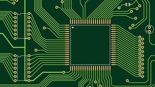
PCB circuit board (high precision impedance circuit board)
④Electrodeposited photoresist film (Electro-deposited Photoresist, ED) is used. Its thickness can be controlled in the range of 5~30/um, which can produce more perfect fine wires. It is especially suitable for narrow ring width, no ring width and full-board electroplating. At present, there are more than ten ED production lines in the world.
⑤ Adopt automatic optical inspection technology (Automatic Optic Inspection, AOI). This technology has become an essential means of detection in the production of fine wires, and is being rapidly promoted, applied and developed. For example, AT&T Company has 11 AoIs, and }tadco Company has 21 AoIs specially used to detect the graphics of the inner layer.
(2) The functional holes of printed circuit boards for surface mounting of micro-hole technology mainly play the role of electrical interconnection, which makes the application of micro-hole technology more important. Using conventional drill bit materials and CNC drilling machines to produce tiny holes has many failures and high costs. Therefore, the densification of printed boards is mostly due to the densification of wires and pads. Although great achievements have been made, its potential is limited. To further improve the densification (such as wires smaller than 0.08mm), the cost is urgent. liters, thus turning to the use of micropores to improve densification.
In recent years, breakthroughs have been made in CNC drilling machine and micro-drill technology, so micro-hole technology has developed rapidly. This is the main prominent feature in current PCB production. In the future, the technology of forming tiny holes will mainly rely on advanced CNC drilling machines and excellent tiny heads, while the holes formed by laser technology are still inferior to those formed by CNC drilling machines from the point of view of cost and hole quality.
①There are indeed many problems in drilling tiny holes with conventional CNC drilling machines and drills. It has hindered the progress of micro hole technology, so laser hole etching has been paid attention, research and application. But there is a fatal disadvantage, that is, the formation of horn holes, which is aggravated with the increase of plate thickness. In addition to the pollution of high temperature ablation (especially for multi-layer boards), the life and maintenance of the light source, the repeatability of the etching hole and the cost, the promotion and application of micro holes in the production of printed boards has been limited. However, laser etching is still used in thin and high-density microplates, especially in MCM-L's high-density interconnect (HDI) technology, such as polyester film etching and metal deposition (sputtering) in M.C.Ms. technology) combined with high-density interconnection. The formation of buried vias in high-density interconnect multilayer circuit boards with buried and blind via structures can also be applied. However, due to the development and technological breakthroughs of CNC drilling machines and tiny drill bits, they have been rapidly promoted and applied. Thus the laser drilled holes on the surface
The application in the mounted circuit board cannot form a dominant position. But it still has a place in a certain field.
② CNC drilling machine At present, the technology of CNC drilling machine has made new breakthroughs and progress. And formed a new generation of CNC drilling machine characterized by drilling tiny holes. The efficiency of drilling small holes (less than 0.50mm) by the micro-hole drilling machine is 1 times higher than that of the conventional CNC drilling machine, with fewer failures, and the rotation speed is 11-15r/min; it can drill 0.1-0.2mm micro-holes, and the cobalt content is higher. The high-quality small drill bit can stack three plates (1.6mm/piece) for drilling. When the drill bit is broken, it can automatically stop and report the position, automatically replace the drill bit and check the diameter (the tool magazine can hold as many as hundreds), and can automatically control the constant distance between the drill tip and the cover plate and the drilling depth, so blind holes can be drilled. , and will not damage the countertop. The CNC drilling machine table adopts air cushion and magnetic floating type, which moves faster, lighter and more precise, and will not scratch the table. Such drilling machines are in short supply at present, such as the Mega4600 from Prurite in Italy, the ExcelIon2000 series in the United States, and new-generation products from Switzerland and Germany.
③Buried, blind, through-hole technology Buried, blind, through-hole technology is also an important way to improve the high density of printed circuits. Generally, buried and blind vias are tiny holes. In addition to increasing the number of wirings on the board, buried and blind vias are interconnected between the "nearest" inner layers, which greatly reduces the number of through holes formed, and the setting of the isolation disc will also greatly reduce the number of vias. Reduced, thereby increasing the number of effective wiring and interlayer interconnections in the board, and improving the high density of interconnections. Therefore, the multi-layer circuit board with the combination of buried, blind and through-hole is at least 3 times higher than the conventional all-through-hole board structure under the same size and number of layers. The size of the printed board combined with the through hole will be greatly reduced or the number of layers will be significantly reduced. Therefore, in high-density surface mount printed boards, buried and blind via technologies are increasingly used, not only in surface mount printed boards in large computers, communication equipment, etc., but also in civil and industrial applications. It has also been widely used in the field of , and even in some thin boards, such as various PCMCIA, Smard, IC cards and other thin boards with more than six layers.
The printed circuit boards with buried and blind hole structures are generally completed by the "split board" production method, which means that it can only be completed after many times of pressing, drilling, hole plating, etc., so precise positioning is very important. .
Read recommendations:
Single-sided double-layer AL base PCB
Aluminum substrate (double-sided)
Six-layer Immersion Gold Board (BGA)
Gigabit Ethernet PCB Layout Guidelines.Electronic Manufacturing Services PCB
Popular recommended products
Six-layer Immersion Gold Board (BGA)
2021-04-27Mobile phone template (six layers)
2021-04-27Six-layer Immersion Gold Board (BGA)
2021-04-27High frequency PCB
2021-04-27Six-layer Immersion Gold Board (BGA)
2021-04-27Laminate copper-based PCB after 4L (sample)
2021-04-27Network communication board (sixth floor)
2021-04-29High frequency PCB
2021-04-27Six-layer Immersion Gold Board (BGA)
2021-05-24Silver oil perforated plate (double-sided)
2021-04-27Six-layer Immersion Gold Board (BGA)
2021-04-27High frequency PCB
2021-04-27Computer card board (four layers)
2021-04-25Single copper base PCB
2021-04-27Six-layer Immersion Gold Board (BGA)
2021-05-24Single-sided double-layer AL base PCB
2021-04-27Six-layer Immersion Gold Board (BGA)
2021-05-27High frequency PCB
2021-04-27Six-layer Immersion Gold Board (BGA)
2021-05-27Six-layer Immersion Gold Board (BGA)
2021-05-27Display board (six layers)
2021-04-27Six-layer Immersion Gold Board (BGA)
2021-05-27Aluminum substrate (double-sided)
2021-04-27Mobile phone board
2021-04-27SMT stickers
2021-05-27SMT stickers
2021-05-27Six-layer Immersion Gold Board (BGA)
2021-04-26Mobile phone board
2021-05-27DIP plugin
2021-05-27Six-layer Immersion Gold Board (BGA)
2021-04-26Six-layer Immersion Gold Board (BGA)
2021-04-26Six-layer Immersion Gold Board (BGA)
2021-04-26DIP plugin
2021-05-27Six-layer Immersion Gold Board (BGA)
2021-04-26Related Information
The relationship between PCB safety distance and voltage
2024-04-22SMT surface mount processing.Hybrid circuit board PCB
2024-04-15PCB enterprises should pay attention to SMT matters.Electronic components PCB
2024-04-03PCB - the core building block of electronic products.Automotive Electronics PCB
2024-03-25PCB - the bridge and link of the electronic world
2024-03-18How to define high-frequency and high-precision circuit boards.Industrial Electronics PCB
2024-03-11USB PCB interface layout and wiring requirements
2024-01-22Electrolytic capacitor PCB.Steps for using PCB pins
2024-01-15Automotive ElectronicWhat aspects should be considered when processing and manufacturing PCB boards?
2024-01-08Electrolytic capaciWhat is the difference between a gold-plated circuit board and a gold-plated one?
2023-12-25When grinding PCB boards, attention should be paid to.Oscillator (belonging to crystal) PCB
2023-12-18Industrial Electronics PCB!What precautions should be taken when copying and grinding PCB boards
2023-12-11Do you know who is more suitable for LED direct display, regarding the difference between PCB board
2023-12-05Aluminum electrolytic capacitor PCB.What are the standards for selecting PCB boards
2023-11-27Surface Mount Technology (SMT) Phase PCB
2023-11-20Oscillator (belonging to crystal) PCB.The main functions of PCB board
2023-11-13What is the difference between RO filter and PCB filter
2023-11-06Method for determining blind hole PCB board
2023-11-01Electronic Manufacturing Services PCB!What are the effects of PCB board color on performance?
2023-10-23Introduction to the Manufacturing Steps and Requirements of PCBA Test Stand
2023-10-16PCB version maturity stage.AOI circuit board price
2023-09-25How to maintain a PCB circuit board
2023-09-19Development Trend of Printed Circuit Board.Zener diode PCB Vendor
2023-09-14Common problems and cause analysis of PCB circuit board sampling.Zener diode PCB price
2023-09-08What are the issues that need to be understood in PCB circuit board design?IGBT module PCB factory
2023-09-08How to reduce the risk of bending and deformation in PCB circuit board production?Inverter PCB Produ
2023-08-16What are the three main factors that constitute welding defects in PCB circuit boards?Multilayer PCB
2023-08-16The structure of a glass teapot.LCD Module PCB factory
2023-08-11Glass teapot.Inverter PCB Processing
2023-08-11PCB online debugging
2023-08-08
CopyRight © 2007-2024Shenzhen Weienchen Technology Co., Ltd.
粤ICP备2021061255号

Address:
1205, Floor 12, Building 3, Chuangyi Office Building, No. 110, Ziheng West Road, Jinsha Community, Kengzi Street, Pingshan District, Shenzhen, Guangdong, China

Tel:
+86-755-29662580

Email:
sales@victoriapcb.com

PCB

PCBA
Service
Process
 Tel: +86-755-29662580
 Email: sales@victoriapcb.com
 中
中 current position:


